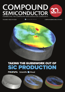
We are proud to announce that the SiC Puck Scanner, co-authored by PVA TePla and Scientific Visual, is featured on the cover of Compound Semiconductor (Vol. 31, Issue VIII 2025) — one of the most respected publications in the semiconductor industry.
The cover story, titled “Taking the Guesswork out of SiC Production,” highlights how the new inspection solution revolutionizes quality control in SiC manufacturing.
By visualizing internal defects in 3D before any slicing, the system helps manufacturers:
-
Eliminate uncertainty in crystal grading
-
Preserve up to 60 % of wafering costs by avoiding defective material
-
Shorten growth feedback loops from weeks to hours
-
Optimize slicing strategy using YieldPro™ Smart Wafering software
“This collaboration with PVA TePla represents a new standard for process transparency in SiC production — enabling faster decisions and higher yield from every crystal,” says Ivan Orlov, CEO of Scientific Visual.
The full article is available online at Compound Semiconductor magazine, and celebrates the growing partnership between PVA TePla Metrology Systems and Scientific Visual in driving smart, data-driven SiC manufacturing.

