What crystals do you need to inspect?
- Tailored for crystals up to 400 kg or ⌀22", in any shape
- 4-axis scanning
- Optimises core positioning for maximum yield
- Outputs G-code for CNC coring systems
- Suited for KY, HEM, CZ and other industrial crystals requiring precision metrology
- Optimised for inspecting raw boules and cylinder ingots up to ∅8"
- Automatic defect detection in crystal volume
- Indicates defect-free zones in mm
- Predicts quality grades (TUA, TUV) of wafers for precise go/no-go decisions
- Automated inspection system for polished and non-polished watch covers
- Ensures only defect-free covers proceed to grinding and polishing, reducing costs
- Up to 1M pieces per year throughput
- Auto-classifies defects such as bubbles, clouds and structures.
- Advanced 3D software for detailed metrology visualisation
- Designed for optical and acoustic (SAM) scanners
- Inscribe cores, wafers and custom 3D shapes in crystal volume to avoid defects and maximise yield
- Send G-code to CNC processing equipment.
Ecological impact of a sapphire cover on a typical Swiss mechanical watch
Presentation of Frédéric Falise at the International Congress of Chronometry 2022 (in french).
Sapphire is an essential component of modern watches because of its exceptional hardness. However, it also makes its processing very energy-intensive. In addition, only about one third of the volume of crystal produced is transformed into final parts. This year-long study reveals that the sapphire cover accounts for up to 88% of the total energy and CO2 of watch manufacturing. Frédéric Falise of Scientific Visual presents the results of the study and solutions for the watch industry to reduce its environmental footprint.
Media contact: media@scientificvisual.ch
| Download presentation |
| Download Scientific Visual article |
| Download Le Temps publication |
Taking guesswork out of crystal production
Scientific Visual offers quality control scanners that visualise volume defects, such as bubbles, cracks and cloudiness, in raw crystals.
They identify imperfections in pre- and post- polished sapphire, ruby, glass, fluorites, SiC and multitude of semiconductor crystals.
Our scanners ensure that only the best quality material enters the costly processing stream. The quality grades are adaptable to customers’ needs.
Scientific Visual services three key markets: watch, semiconductor and smartphone manufacturers.
| Download the flyer ”SapphiroScan™ for the watch industry” |
Automated crystal metrology: Key steps in 90 seconds
Walk through the automated metrology of a 90-kg Kyropolous-grown sapphire boule – from 3D scanning and defect detection to CNC coring. Now with crystal skin texture capture.
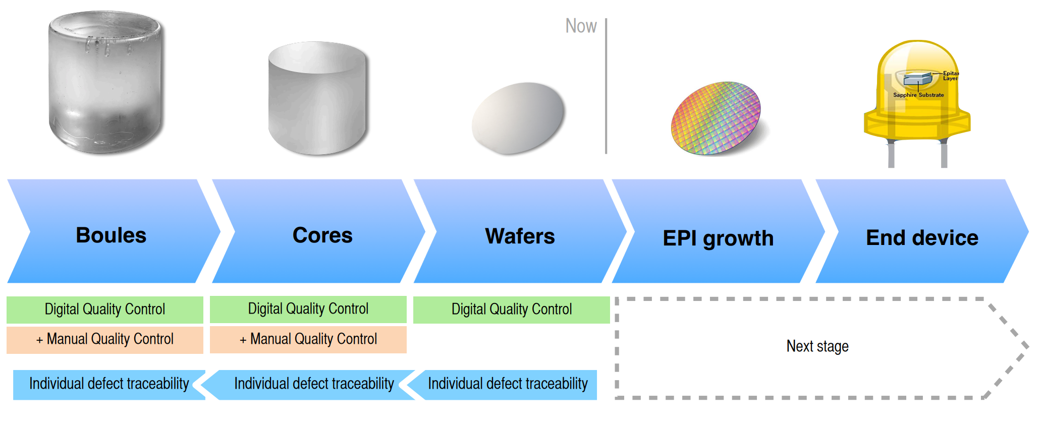
Scientific Visual published a case study: tracking sapphire defects across micro-LED production chain
How to get more quality wafers from the same crystal?
What if you could see internal flaws in sapphire crystal before processing it?
This movie recorded with CarrotScan™ shows defects in a raw sapphire crystal grown by Verneuil method. Scene switches from Skin visualization to Inside view of defects. Colour stands for sapphire defect density: from deep blue (non-defective material) to deep red (highest defectiveness).
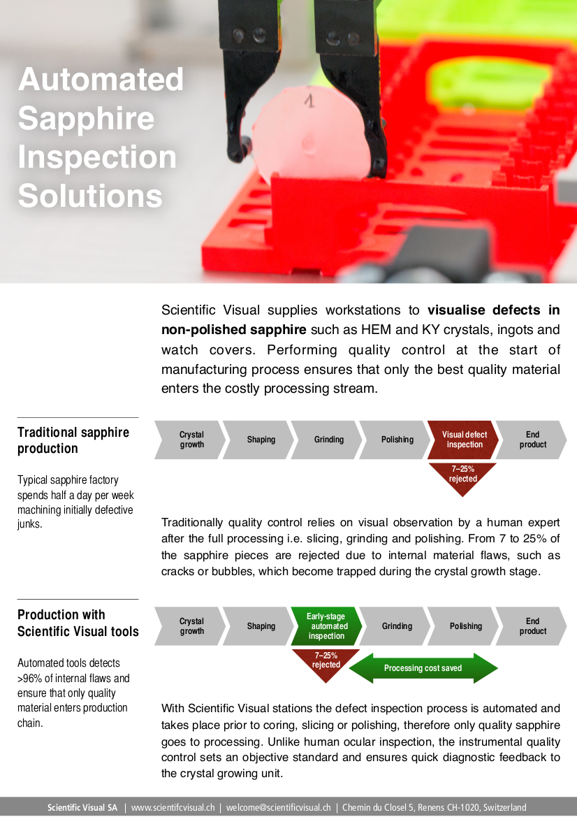
Currently checking for defects in sapphire watch covers and wafers is done after full processing and polishing has been completed.
Today 15-20% of sapphire covers and wafers are rejected after being processed and polished to transparency due to internal flaws that were initially there.
Think about it.
It means that a typical sapphire factory wastes at least 1 day per week polishing discards!
Our SapphiroScan™ control system detects flaws in non-processed watch covers so that only high-quality items could enter the value chain. Providing ROI in 6-18 months, the scanner not only improves quality and reduces production costs, but also accumulates defect statistics for the growth process optimisation.
For Kyropolous and HEM crystal growers SapphiroScope™ automated station offers a fast, highly cost-effective alternative to manual quality control.
Unlike human inspection, all Scientific Visual scanners can be calibrated to perform objectively at a customer standards so ensuring quick, accurate diagnostic feedback during and after production.
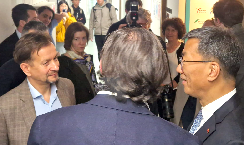
Dr. Huai Jinpeng, Minister of Education of China has visited Scientific Visual
23.03.2026 – Our team was honoured to welcome Minister Huai Jinpeng and his delegation to Scientific Visual.
Video: Smart Wafering lecture at SEMICON Europa
A 4-min explainer of Smart Wafering method to achieving production increase without growing more crystals.

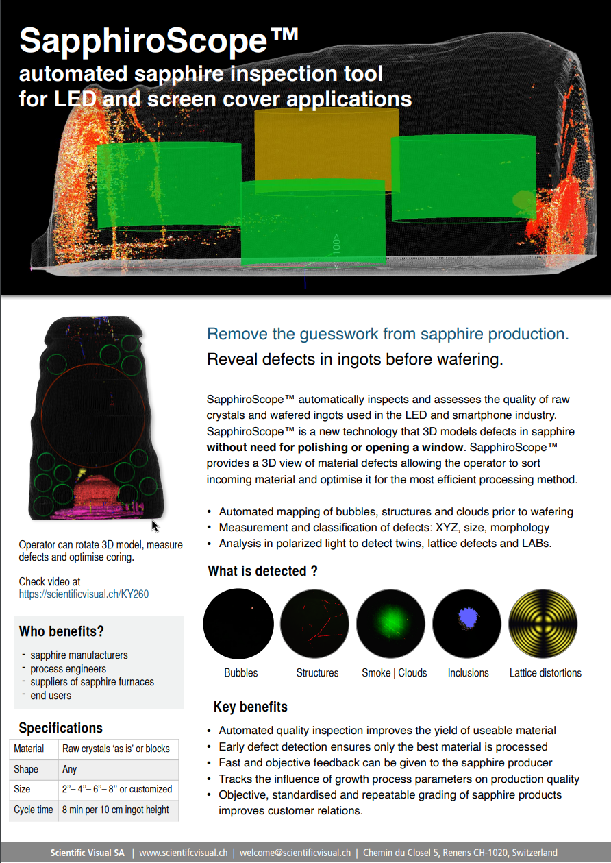
| Download the flyer ”SapphiroScope™ for LED and screen cover applications” |


