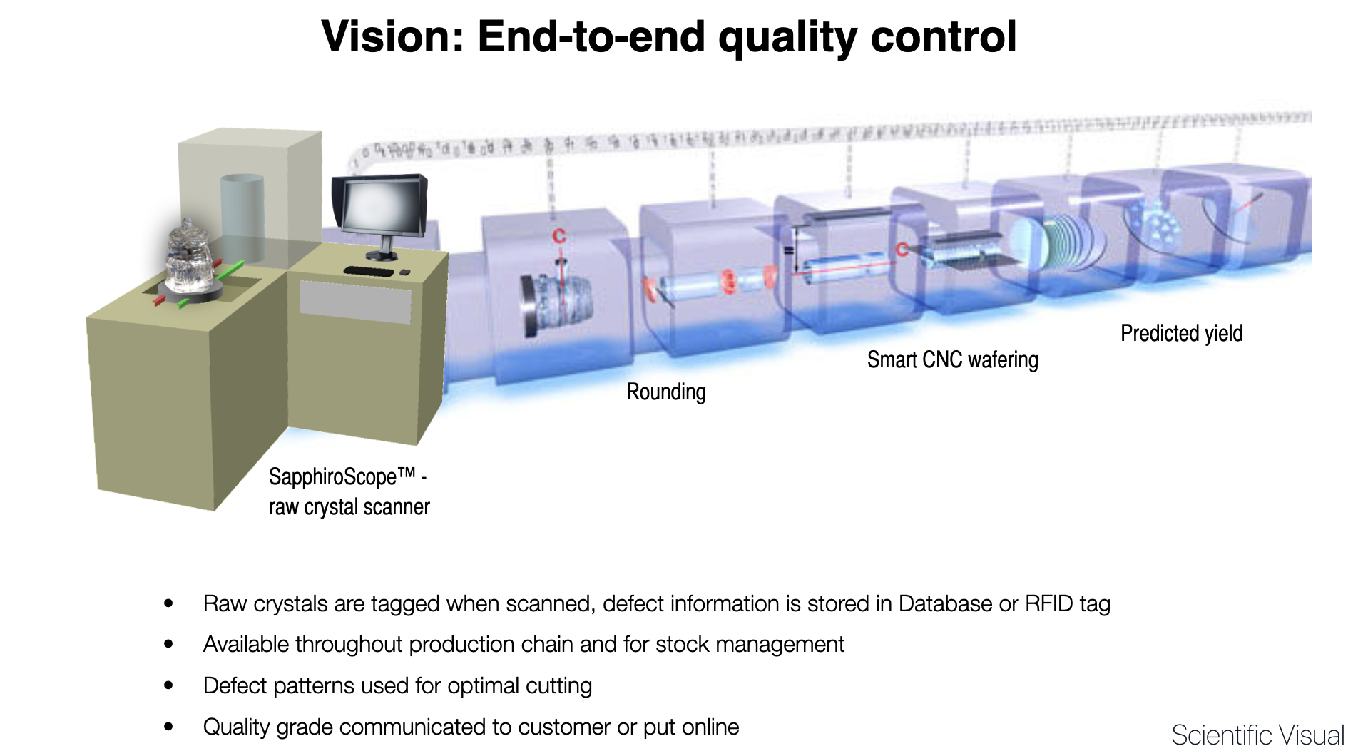
Relevant equipment
SapphiroScope™ – for KY, HEM and EFG ingots for LED and optics up to 12 inches.
Increasing the harvesting yield when processing raw Sapphire Boules into wafers is paramount for the industry. Our technology augments the yield at each processing stage and therefore contributes to the virtuous circle of reducing energy consumption from the growth stage until the end-users:
- At the crystal growth stage by understanding the positive and negative influence of each furnace growth parameter on the formations of defect
- At the crystal processing stages from Boules to Ingots and from Ingots to Wafers. The cutting plan can be optimized by knowing exactly the morphology and location of each defect.
- By avoiding grinding, polishing un-qualified material
- By increasing the quality of the wafer substrate and therefore reducing final dies quality issues
- By increasing the final LED production yield and, therefore, increasing the adoption of low consumption lights it will reduce the amount of energy used by society.
Furthermore, the Sapphire industry will need to meet the industry 4.0 to satisfy with the quality required for Micro-LED production. Our technology is the key enabler to meet today and future quality requirements.

