![]() This project has received funding from the European Union’s Horizon 2020 research and innovation
This project has received funding from the European Union’s Horizon 2020 research and innovation
programme under the Marie Sklodowska-Curie grant agreement No 101033102.
Why is Gallium Nitride (GaN) important?
Gallium Nitride and its related alloys with Indium (In) and Aluminium (Al) are versatile materials that are commonly used for optoelectronic applications such as high brightness light-emitting diodes (LED) and laser diodes. This is because their emission wavelength covers a wide spectral range from the deep ultraviolet (DUV), through the visible to the near-infrared as shown on the figure below.1, 2, 3 In the 2020-2021 pandemic circumstances, irradiation with AlGaN-based DUV LEDs even proved very useful as a sterilization source to inactivate SARS-CoV-2.4 Owing to its wide bandgap as well as high values of electron velocity, breakdown field strength, and thermal conductivity, GaN is also very attractive for high frequency and high power electronics,5 such as 5G phone base chargers.6 As the seek for increased efficiency, power savings, and cost reduction is driving the industry, improving the production of larger GaN substrates with high structural quality is imperative.
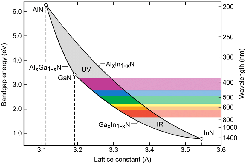
Band gap energy as a function of the lattice constant for group III-nitride alloys at room temperature (Extracted from E. F. Schubert, Light-Emitting Diodes. Cambridge University Press, 2006).
GaN growth
The high GaN melting temperature (above 2200°C) and the need for a nitrogen pressure higher than 6 GPa to enable congruent melting have hindered the production of native GaN wafers.7 However, growing GaN on foreign substrates (known as heteroepitaxy) usually yields higher defectiveness of the crystals due to the deleterious effects of lattice-mismatch and thermal expansion difference. Only very recently bulk GaN substrates with structural quality and dimensions relevant for the industry were made commercially available, driven by the demand from the laser diode market. GaN bulk crystals (see figure below) are presently fabricated by three main methods:
- Vapour Phase Epitaxy (Halide-VPE, Oxide-VPE and Halide Free-VPE),
- Na-flux technology,
- Ammonothermal growth.
As these three techniques run at lower pressure and temperature than the extreme conditions mentioned above, ongoing efforts are being deployed to develop crystal growth processes that yield GaN substrates with diameter larger than 2” and threading dislocation density as low as possible.8 Currently, the lowest value is 10²/cm².
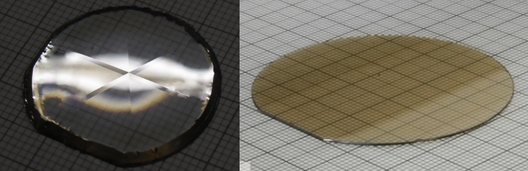
Left: As-grown 1-inch GaN bulk crystal grown by Halide-VPE (Courtesy of T. Sochacki, Institute of High Pressure Physics, Polish Academy of Sciences (IHPP PAS)). Right: A polished 2-inch GaN wafer produced by ammonothermal method (Courtesy of R. Kucharski, IHPP PAS).
Market evolution
The Gallium Nitride market shows steady growth since its first device in 1993. GaN development directly aligns with the European Commission recognition that Advanced Manufacturing Technologies is a key to industrial competitiveness, growth and job creation in Europe.
The GaN power market thrives after its adoption in mobile phone fast charger application where reducing time has become crucial for the 5G push and the demand for extending battery life. In early 2020, OEMs opted for a GaN-based inbox fast charger for their flagships released where high power density, high efficiency and small form factor are needed.
According to a report of the market research company Yole Development done in May 2020, the total radio-frequency GaN market should increase to more than USD 2 billion by 2025, with a compound annual growth rate (CAGR) 12%.9 Moreover, even though US–China conflict related to sanctions toward Huawei, and the COVID-19 outbreak have modified the semiconductor industry landscape, GaN deployment in the telecom keeps growing for the long term.
In January 2021, Fortune Business Insights10 estimated that demand for gallium nitride devices is witnessing an unprecedented and positive impact from COVID-19 across all regions. The global GaN device market will exhibit a growth of 1.03% in 2020 compared to the average year-on-year growth during 2016-2019. The market is projected to grow from USD 21.18 billion in 2020 to USD 28.40 billion in 2027 at a CAGR of 4.28% in the 2020-2027 period.
Towards defect-free production
Оne of the biggest hurdles in the wide-spread use of GaN is to manufacture large diameter defect-free wafers. Even the tiniest crystal defects negatively affect the brightness, output power and lifetime of the electronic devices. Despite ongoing efforts of GaN growers to overcome the occurrence of a high number of defects in crystals, the defectiveness problem remains very acute, principally for two reasons:
- The GaN crystal growth process is challenging to control in real-time. The smallest instability in growth process (such as 1-2°C temperature deviation) could create threading dislocations (see figure below), voids, and cracks during the crystal formation.
- The current defect identification takes place after a time-consuming crystal wafering and polishing procedure. It means that initially, defective areas are wafered and polished and then rejected by downstream quality control. The industry requires a non-destructive quality control tool that could indicate imperfect crystals regions to avoid costly processing and reduce fabrication costs.
Scientific Visual is working to create such an early-stage inspection system to visualize defects in raw GaN crystals. We will publish project news on this page. Our expert staff is happy to test your samples and to apply early-stage inspection technology to your production. Please contact us at your earliest convenience at welcome@scientificvisual.ch.
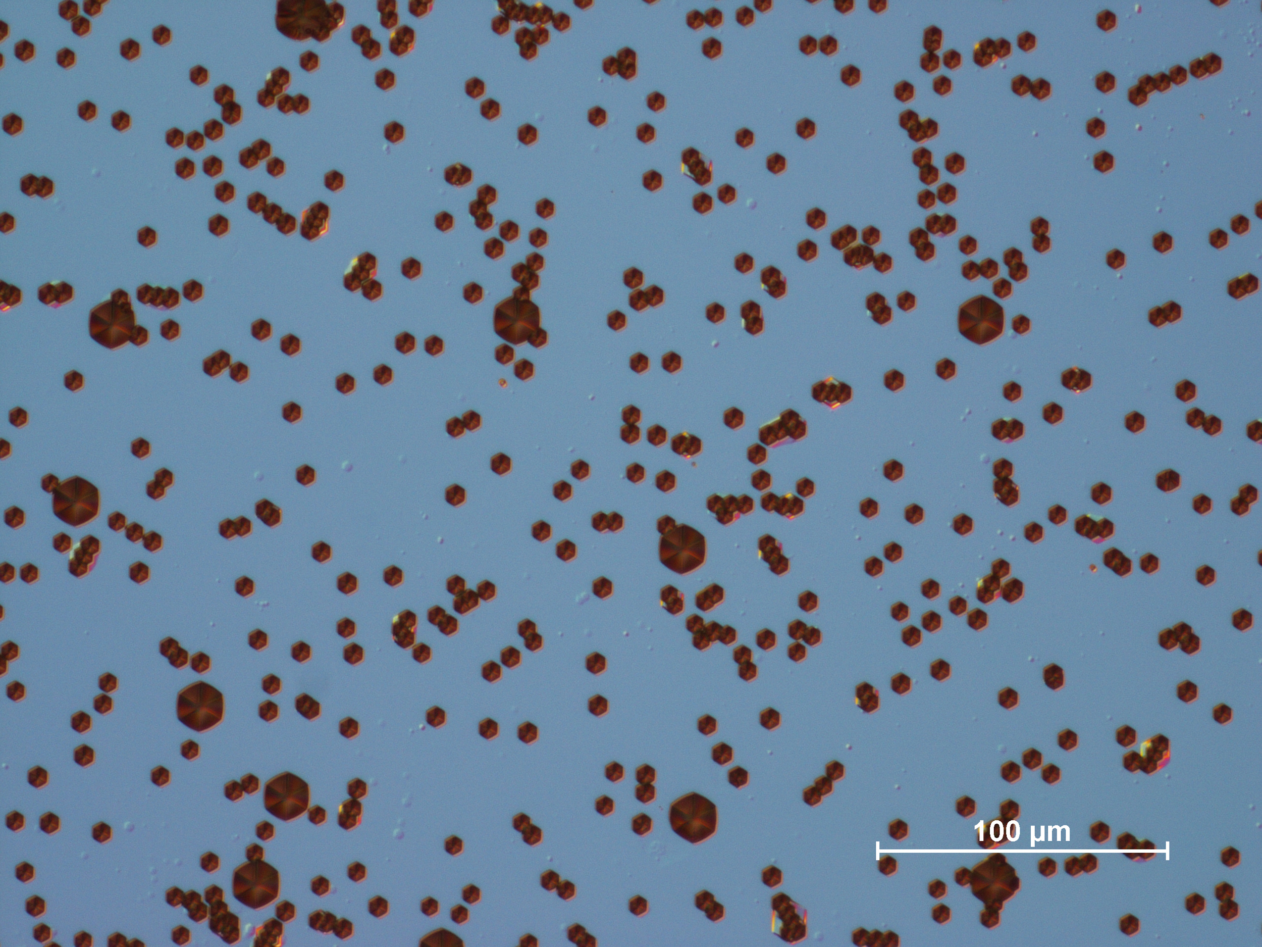
A GaN wafer surface after the defect selective etching (Courtesy of J.L. Weyher, IHPP PAS).
References
- Andreev BA, Kudryavtsev KE, Yablonskiy AN, Lobanov DN, Bushuykin PA, Krasilnikova LV, et al. Towards the indium nitride laser: obtaining infrared stimulated emission from planar monocrystalline InN structures. Sci Rep. 2018 Dec;8(1):9454.
- Ponce FA, Bour DP. Nitride-based semiconductors for blue and green light-emitting devices. Nature. 1997 Mar;386(6623):351–9.
- Kneissl M, Seong T-Y, Han J, Amano H. The emergence and prospects of deep-ultraviolet light-emitting diode technologies. Nat Photonics. 2019 Apr;13(4):233–44.
- Liu S, Luo W, Li D, Yuan Y, Tong W, Kang J, et al. Sec‐Eliminating the SARS‐CoV‐2 by AlGaN Based High Power Deep Ultraviolet Light Source. Adv Funct Mater. 2021 Feb;31(7):2008452.
- Baron N. Power GaN. Patent lanscape. Yole Developpement; 2019 Nov. Available from: https://www.knowmade.com/downloads/power-gan-patent-landscape/
- Kareta N. GaN takes over mobile device charging. Available from: https://www.power-and-beyond.com/gan-takes-over-mobile-device-charging-a-939854/
- Utsumi W, Saitoh H, Kaneko H, Watanuki T, Aoki K, Shimomura O. Congruent melting of gallium nitride at 6 GPa and its application to single-crystal growth. Nat Mater. 2003 Nov;2(11):735–8.
- Kucharski R, Sochacki T, Lucznik B, Bockowski M. Growth of bulk GaN crystals. J Appl Phys. 2020 Aug 7;128(5):050902.
- GaN RF Market: Applications, Players, Technology and Substrates 2020. i-Micronews.com. 2020. Available from: https://www.i-micronews.com/products/gan-rf-market-applications-players-technology-and-substrates-2020/?utm_source=PR&utm_medium=email&utm_campaign=PR_RF_GaN-MarketUpdate_YOLE_May2020
- Gallium Nitride (GaN) Device Market Size, Share & Forecast, 2027. Available from: https://www.fortunebusinessinsights.com/gallium-nitride-gan-devices-market-103367